Transparent Electronics: 45 Percent Transparency achieved in Microdisplays
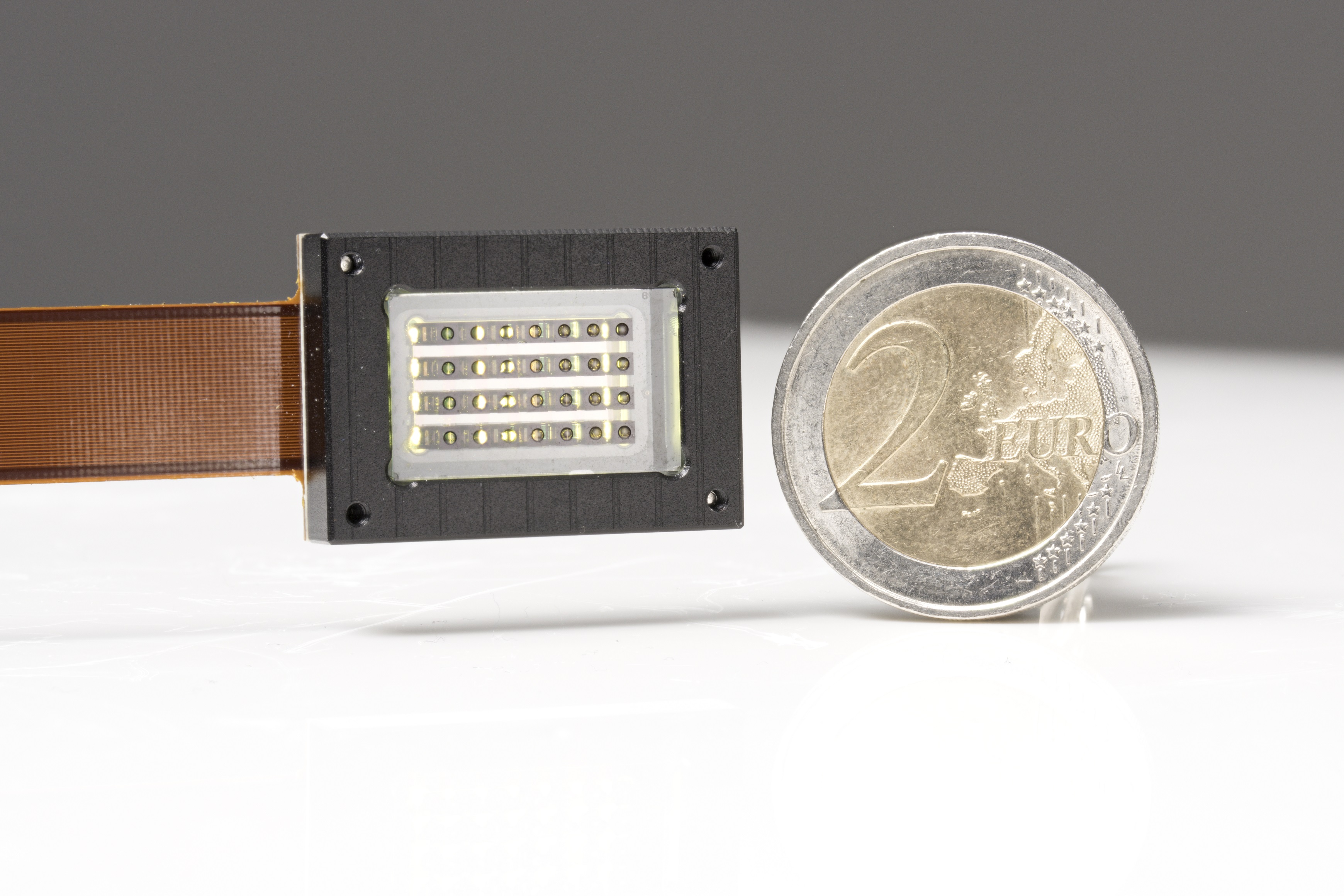
Researchers from the Fraunhofer Institute for Photonic Microsystems IPMS have significantly increased the transparency of OLED microdisplays. For the first time, a microdisplay of this kind will be presented at booth No. 38 at the "International Meeting on Information Display" (IMID) 2024 in Jeju, South Korea.
Transparent electronics are already providing reliable services in some applications. For instance, they can be found as ultra-thin layers for touch displays or as transparent films with printed antennas for mobile communications. However, OLED microdisplays have not been transparent so far.
As part of the HOT project (“High-performance transparent and flexible micro-electronics for photonic and optical applications,” funding number MAVO 840092) funded by the Fraunhofer Society, OLED microdisplays with 20% transparency were developed. The technology has now been advanced further, and for the first time, 45% transparency has been achieved in a CMOS OLED microdisplay.
What causes this improvement?
The OLED-on-silicon technology uses a silicon backplane that contains the entire active matrix drive electronics for the pixels. The organic frontplane is monolithically integrated on the topmost metallization layer, which simultaneously serves as the drive contact for the organic light-emitting diode. The second connection of the OLED is formed by a semi-transparent top electrode shared by all pixels. The pixel circuitry is based on silicon CMOS technology and requires several metal layers to connect the transistors embedded in the substrate. These metal connections are made of aluminum or copper. Additionally, the optical structure of the OLED requires a highly reflective bottom electrode to ensure high optical efficiency upwards. These two aspects result in the pixels themselves not being transparent.
"A transparent microdisplay, however, can be realized through a spatially distributed design of this basic pixel structure, creating transparent areas between the pixels and minimizing column and row wiring," explains Philipp Wartenberg, group leader of IC and system design at Fraunhofer IPMS, "further optimization of the OLED layers, for example by avoiding OLED layers in the transparent areas, introducing anti-reflective coatings, and redesigning the wiring also contributes to increasing transparency."
There are two fundamental methods to achieve semi-transparency in optical systems:
1. Pixel approach: This involves creating transparent areas between individual pixels.
2. Cluster approach: This method groups several pixels into a larger, non-transparent cluster. Larger transparent areas are created between these clusters.
Both approaches are relevant for different applications in practice. The pixel approach is suitable, for example, for image overlay within a complex optical system, where the image is inserted between other image planes.
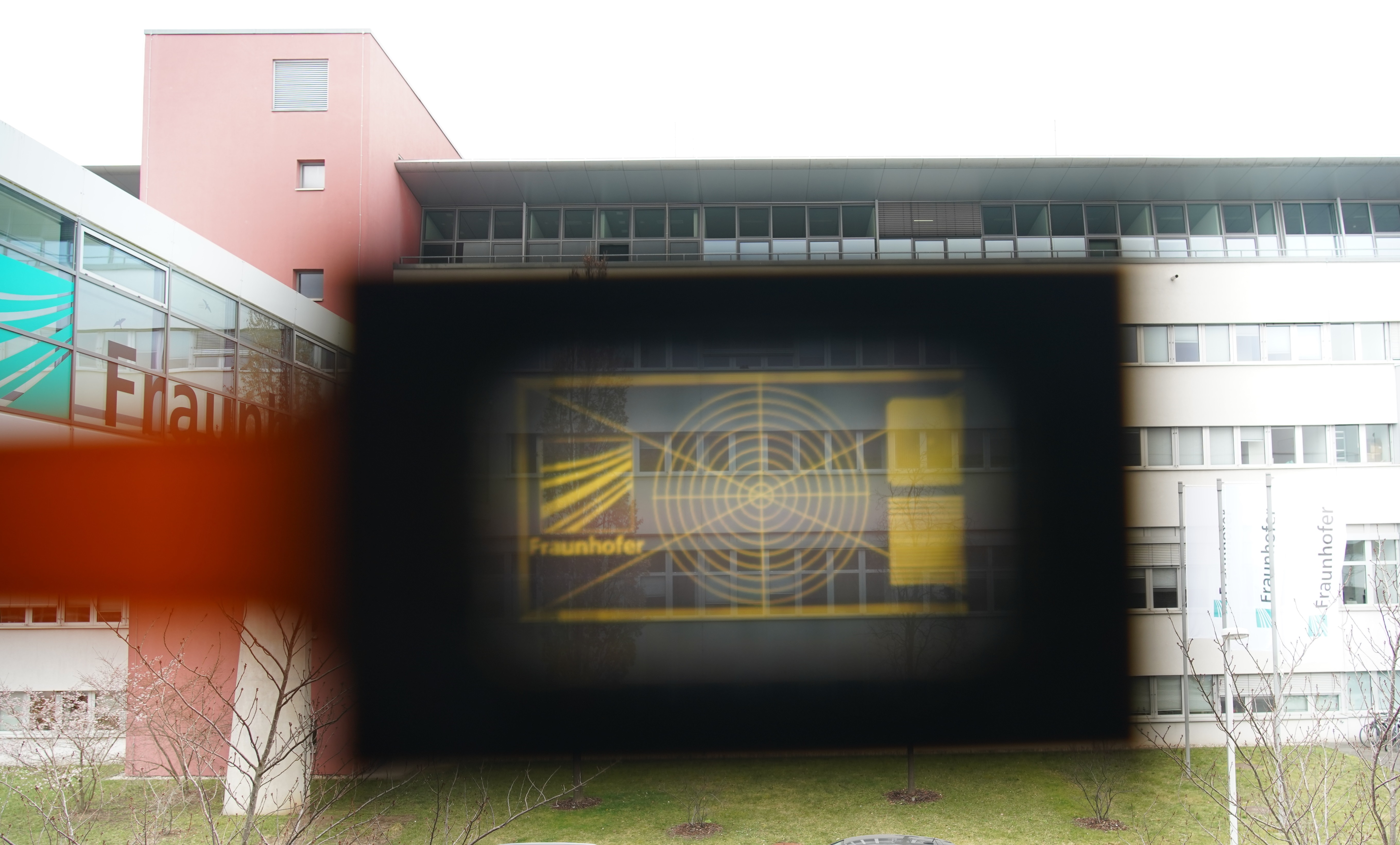
The cluster approach is particularly suitable for augmented reality (AR) applications, such as in data glasses, where the pixel clusters are combined into a uniform virtual image using a micro-optic over each cluster. The transparent areas between the clusters remain unaffected by the optics, allowing a clear view of the real environment.
The technology for transparent microdisplays was developed to support both techniques. The microdisplay presented at IMID showcases the cluster approach with a new AR optic.
Optical Approach
The optical combination of the individual pixel clusters into a uniform virtual image was realized through a microlens array. The optics were designed to enable a setup close to the eye with a similar distance to the eye as regular corrective glasses.
About the HOT Project
(High-performance Transparent and Flexible Micro-Electronics for Photonic and Optical Applications)
This work was funded within a Fraunhofer internal program under funding number MAVO 840092. Additionally, the researchers were supported by Fraunhofer IOF in micro-optics.
About Fraunhofer IPMS
Fraunhofer IPMS is one of the leading international research and development service providers for electronic and photonic microsystems in the application fields of intelligent industrial solutions and manufacturing, medical technology and health, and mobility. In three state-of-the-art clean rooms and with a total of four development sites in Dresden, Cottbus and Erfurt, the institute develops innovative MEMS components and microelectronic devices on 200 mm and 300 mm wafers. Services range from consulting and process development to pilot production.
 Fraunhofer Institute for Photonic Microsystems


