200 mm Cleanroom Infrastructure

© Fraunhofer IPMS
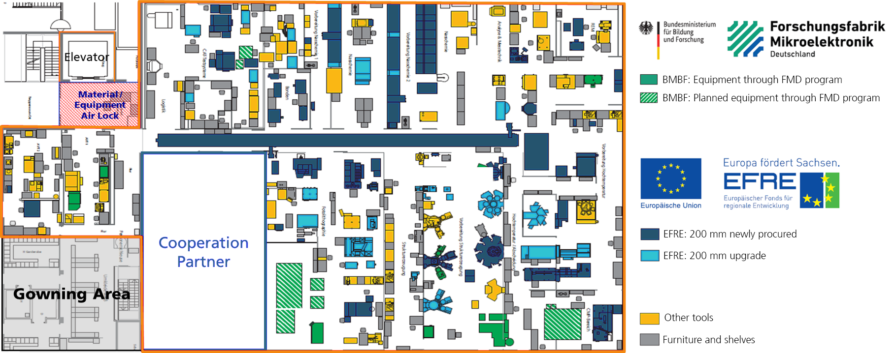
200 mm cleanroom layout at Fraunhofer IPMS:

We offer a state-of-the-art, fully integrated and CMOS-compatible ME(O)MS-on-CMOS line.

Our cleanroom, with its qualified team and industry-oriented facilities, is ideally positioned for research and development in the field of MEMS and MOEMS devices. In addition to a deep understanding of state-of-the-art MEMS manufacturing processes, coupled with modern fab technology, we are the perfect partner for technology and device development.

Our cleanroom at a glance:

  • Low volume & high mix
  • Operation 24/5 in 3 shifts
  • 45 engineers + 45 operators and maintenance technicians
  • ~1,000 wafer starts per month
  • CMOS compatibility
  • Class 10 (ISO 4) on 1,500 m²
  • Certification according to ISO 9001:2015
  • MES for planning, traceability and documentation
  • i-line (400nm L&S) and DUV cluster (130nm L&S)

Lithography

i-Line Stepper

  • 400 nm L / S

DUV-Scanner

  • down to 130/ 110 nm L / S
  • NSR-S210D Hi NA-248 nm Belichtungs-Scanning-System
  • KrF Excimer Laser

Coater

  • Spin
  • Spray

Double-side Mask Aligner

© Fraunhofer IPMS

Dry Etch - (Deep) Reactive Ion Etching

RIE of

  • Oxides
  • Metals
  • Silicon

RIE of Membranes

  • TiAl

DRIE of silicon

  • Aspect ratio up to 40
  • Side wall angle 90° ± 1°
© Fraunhofer IPMS

Wet Etch

Si anisotropic etch (TMA)

  • Membranes
  • Grooves

Al (Phosphoric acid and Acetic acid)

SiO2 (NH4F-buffered HF)

SiN (Phosphoric acid)

© Fraunhofer IPMS

Cleaning

Wafer cleaning

Nanospray, brush, cone brush

Wet stripping (EKC clean)


© Fraunhofer IPMS

Sputtering, Evaporation and ALD

PVD Sputtering:

Interconnectors

  • Al
  • AlSiCu
  • Ti
  • TiN

Chemical Sensors and Barriers

  • Ta
  • Ta2O5
  • HfO2

Mirrors and Hinges

  • Al / Al2O3
  • TiAl
  • Al-Alloys
  • SiO2


Evaporation

  • Al
  • SiO2
  • Al2O3
  • TiO2


ALD

  • FDTS
  • Al2O3
  • HfO2
  • SiO2
© Fraunhofer IPMS

Oxidation, Temperature and CMP

PE-CVD

Dielectrics

  • PE-USG, PE- BPSG
  • SA-USG, HDP-Oxide
  • Si3N4

Silicon and compounds

  • a-Si
  • SiGe

Applications

  • ILD  / Passivation
  • Membranes
  • Construction Layer


LP-CVD

Trenchfill

  • Poly-Si
  • SiO2

Insulator, Membranes

  • Poly-Si
  • SiO2
  • Si3N4


CMP

5-zone CMP

  • Si
  • SiO2


Annealing

Furnace

Rapid Thermal Annealing


Oxidation

Dry, wet

Horizontal, vertical

© Fraunhofer IPMS

Metrology & Inspection

Metrology

Film Thickness Measurement

  • Optical Thickness Measurement
  • In line Reflectance

CD-SEM

Ellipsometer

  • Optical Properties

Defect Measurement

  • Defect Inspection
  • Defect Classifcation  


Inspection

Scanning Electron Microscope

  • 3D Inspection
  • Analysis SEM with FIB cut

Surface Topology Measurement

  • Atomic Force Microscope
  • White Light Interferometer 
  • Laser Scanning Microscope

Actuation Measurement

  • Ultra high frequency vibrometer
© Fraunhofer IPMS

Virtual tour of our 200 mm MEMS cleanroom