 Fraunhofer Institute for Photonic Microsystems
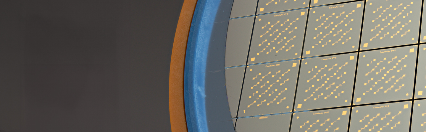
Characterization of Materials
Material characterization of inks and pastes for electrical applications involves analyzing their electrical properties to ensure optimal performance. Key aspects include measuring conductivity and resistivity to determine how well the material can conduct electricity. Dielectric properties, such as dielectric constant and loss tangent, are assessed to understand the material's insulating capabilities. Additionally, the examination of the percolation threshold helps identify the minimum concentration of conductive particles needed for effective conductivity. Thermal and electrical stability are also evaluated under various environmental conditions to ensure reliability. This comprehensive electrical characterization ensures that inks and pastes meet the stringent requirements for use in electronics, printed circuits, and other high-tech applications.
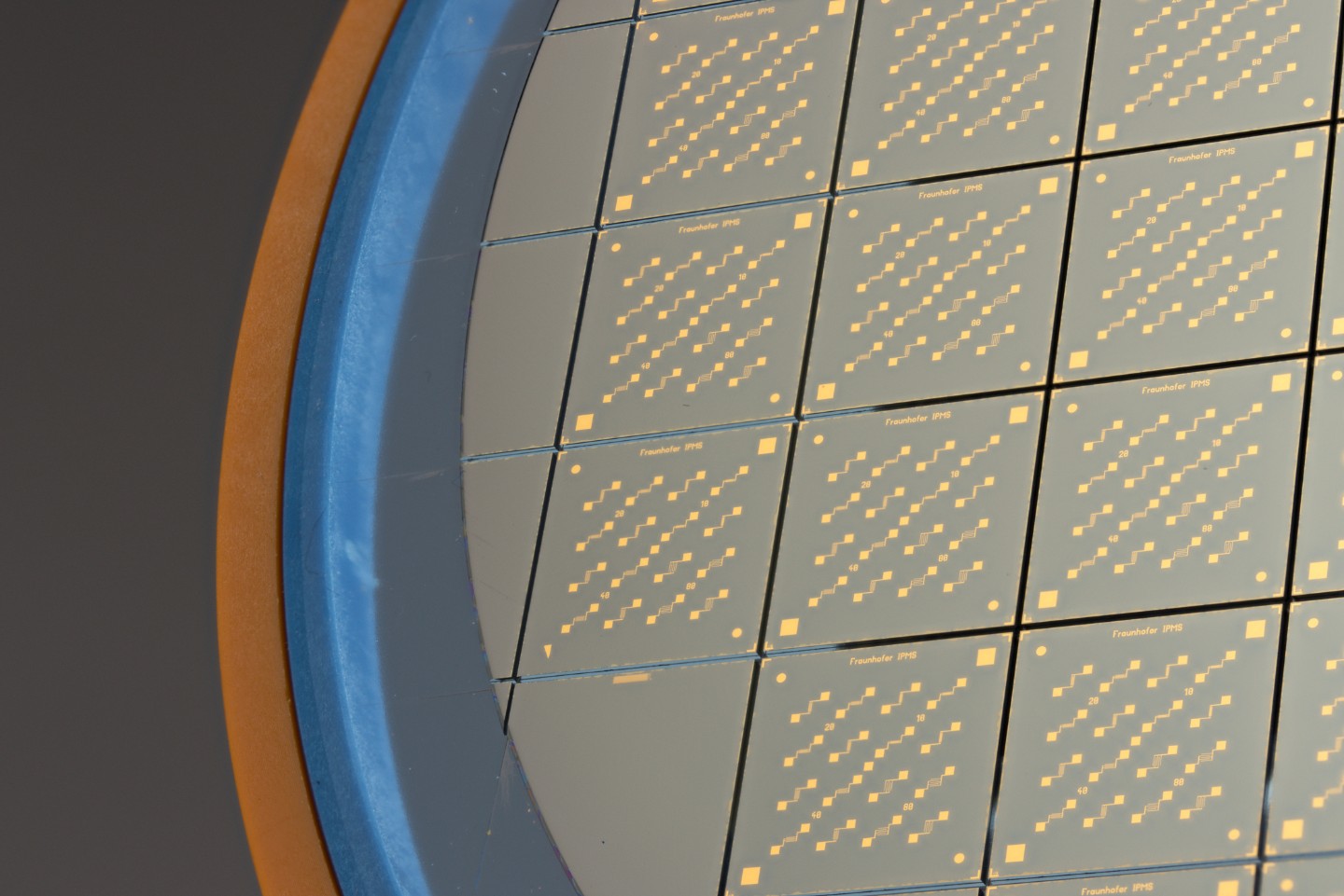
The chip substrates produced at Fraunhofer IPMS offer high-precision structures and high-performance materials, providing a promising basis for reproducible material evaluation in the context of R&D questions and qualification. The substrates offer different customized designs of the electrode structures, e.g. different channel widths and lengths on one chip, so that the ideal parameters can be used for specific applications.
The substrates are regularly fabricated in a clean room on silicon wafers with thermal silicon dioxide (SiO2), with other oxides such as hafnium dioxide (HfO2) available as dielectrics.
In sensor development, the sensitive materials determine the performance of the entire sensor. Material and process developers can apply semiconductor layers to the substrates by solution, chemical vapor deposition (CVD), or physical vapor deposition (PVD). Subsequent electrical characterization allows for characterization and evaluation based on conductivity, carrier mobility, and other performance parameters. As soon as a gas-sensitive material comes into contact with the analyte, this leads to a change in the electrical properties.
The substrates from Fraunhofer IPMS offer a simple way to record these changes. The sensor materials can be evaluated with respect to sensitivity and drift and then optimized, e.g. by adjusting the deposition parameters. Due to the wafer-level manufacturing technology, the substrates are also an interesting basis for product-oriented development.
The test structures can be easily contacted and measured with the specially developed prober.