Organic Electrochemical Transistors (OECTs) and Organic Field-Effect Transistors (OFETs) are both integral components of Organic Thin-Film Transistors (OTFTs). OECTs operate by modulating the conductivity of an organic channel through the electrochemical doping process, which offers high sensitivity and low operating voltages, making them suitable for bioelectronics and sensor applications. In contrast, OFETs control the current flow via an electric field applied through a gate electrode, providing high switching speeds and stability, which are advantageous for display technologies and flexible electronics. While OECTs excel in environments requiring aqueous compatibility and biocompatibility, OFETs are more suited for applications demanding high-speed operation and device integration. They are particularly useful for bioassays and neuromorphic circuits.
In bioassays, OECTs can detect biological signals with high sensitivity, making them ideal for applications such as monitoring glucose levels, detecting pathogens, or measuring neurotransmitter concentrations. In neuromorphic computing, OECTs can mimic the behavior of biological neurons and synapses, offering potential for developing advanced computing systems that replicate brain-like processing.
Arrays of OECTs can be designed to mimic neural networks, facilitating the development of neuromorphic computing systems. These arrays can replicate the behavior of neurons and synapses, enabling advanced computational tasks such as pattern recognition and learning.
Both types of transistors leverage the unique properties of organic materials, offering complementary strengths within the broader category of OTFTs.
Overall, the precise design and selection of electrode materials and geometries are essential for the optimal performance and reliability of OECTs and OFETs within OTFT technology.
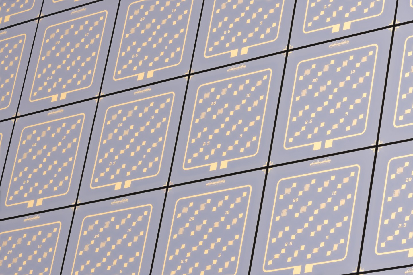
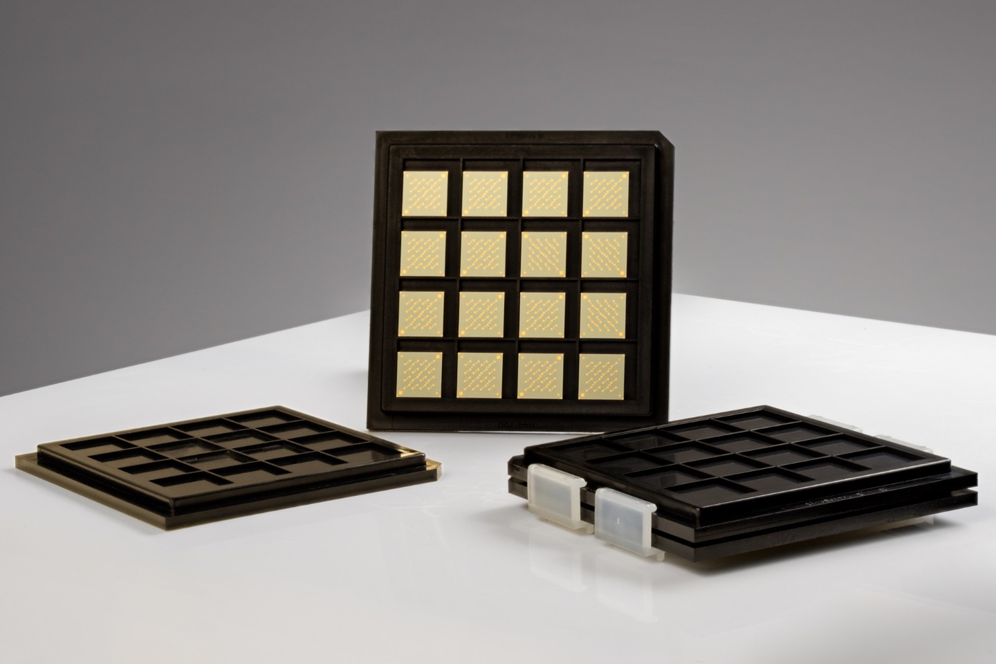
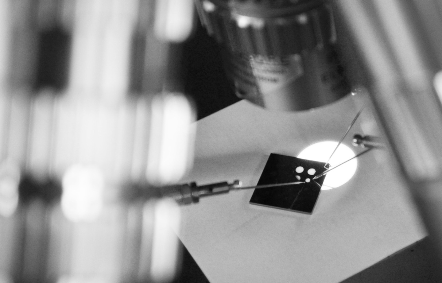
Electrode design plays a crucial role in both OECTs and OFETs, significantly influencing the efficiency and performance of the transistors. In OECTs, the electrodes must not only provide good electrical conductivity but also be biocompatible, especially for applications in bioelectronics. Materials such as gold, platinum, or conductive polymers are commonly used. The surface of the electrodes can be functionalized to enhance interaction with biological molecules.
When using silicon as the substrate for OECTs, it provides a stable and highly reproducible platform that supports precise electrode design. Silicon substrates allow for the integration of microfabrication techniques, enabling the creation of highly reproducible and finely patterned electrodes. This precision in electrode design enhances the performance and sensitivity of the OECTs, saving time and increasing the relevance of the experiments.
 Fraunhofer Institute for Photonic Microsystems