Fraunhofer Institute for Photonic Microsystems
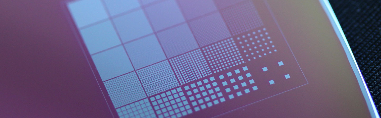
Nanopatterning / E-Beam Lithography
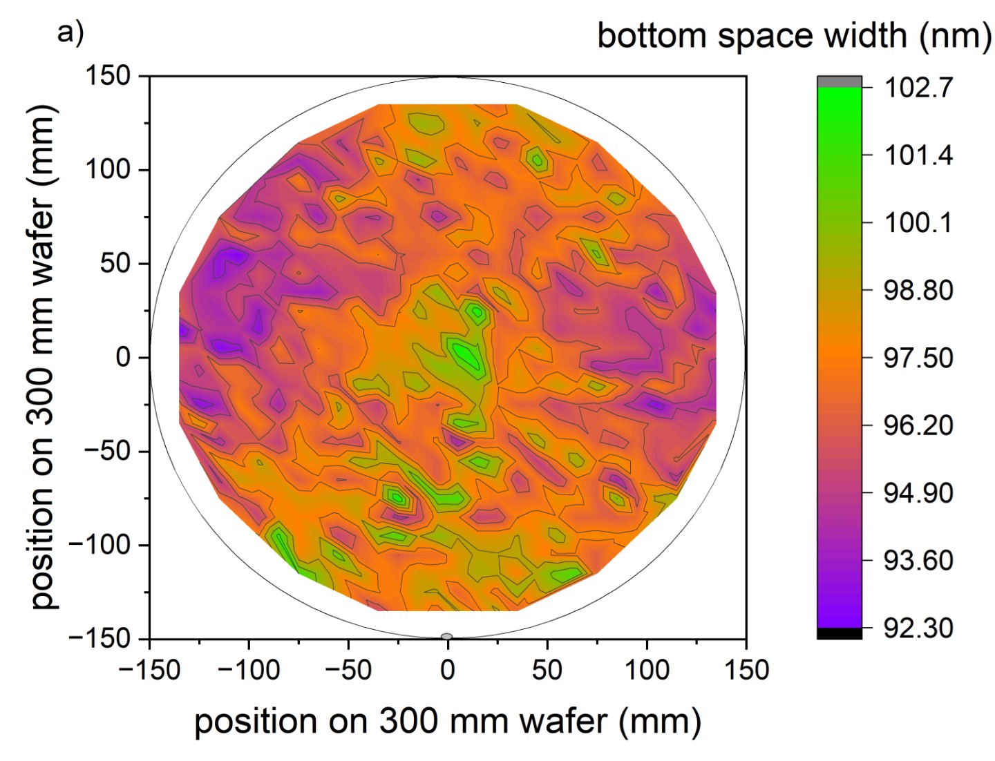
Creating nano-scale structures is crucial for a wide range of applications in the semiconductor business. Key challenges are creating precisely controlled patterns with small dimensions, flexible and adaptable layout generation and processes as well as uniform and reproducible wafer-scale integration.
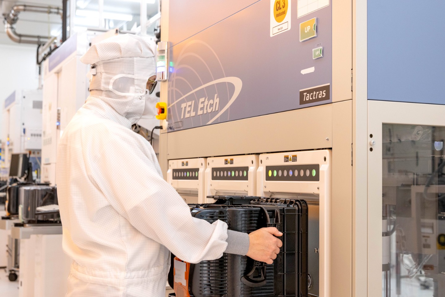
Fraunhofer IPMS offers state-of-the-art nanopatterning capabilities using electron beam direct write lithography and reactive ion etching. Thus, customized structures with sizes below 40 nm can be created on a variety of wafer sizes and substrate types. Starting from the customer’s design the whole package involving layout generation and modification, data preparation, e-beam lithography, pattern transfer using etch processes together with the in-line metrology and analytics up to dicing into single chips is offered.
Application examples
- Fabrication of test structures for technology development
- Structuring of Application Specific Integrated Circuits (ASICS)
- Design tests of innovative devices and cell concepts and their variation on a wafer (Chip Shuttle)
- Calibration pattern for metrology development
- MEMS and NEMS patterning with productive quality
- “Mix & Match” with optical exposure techniques