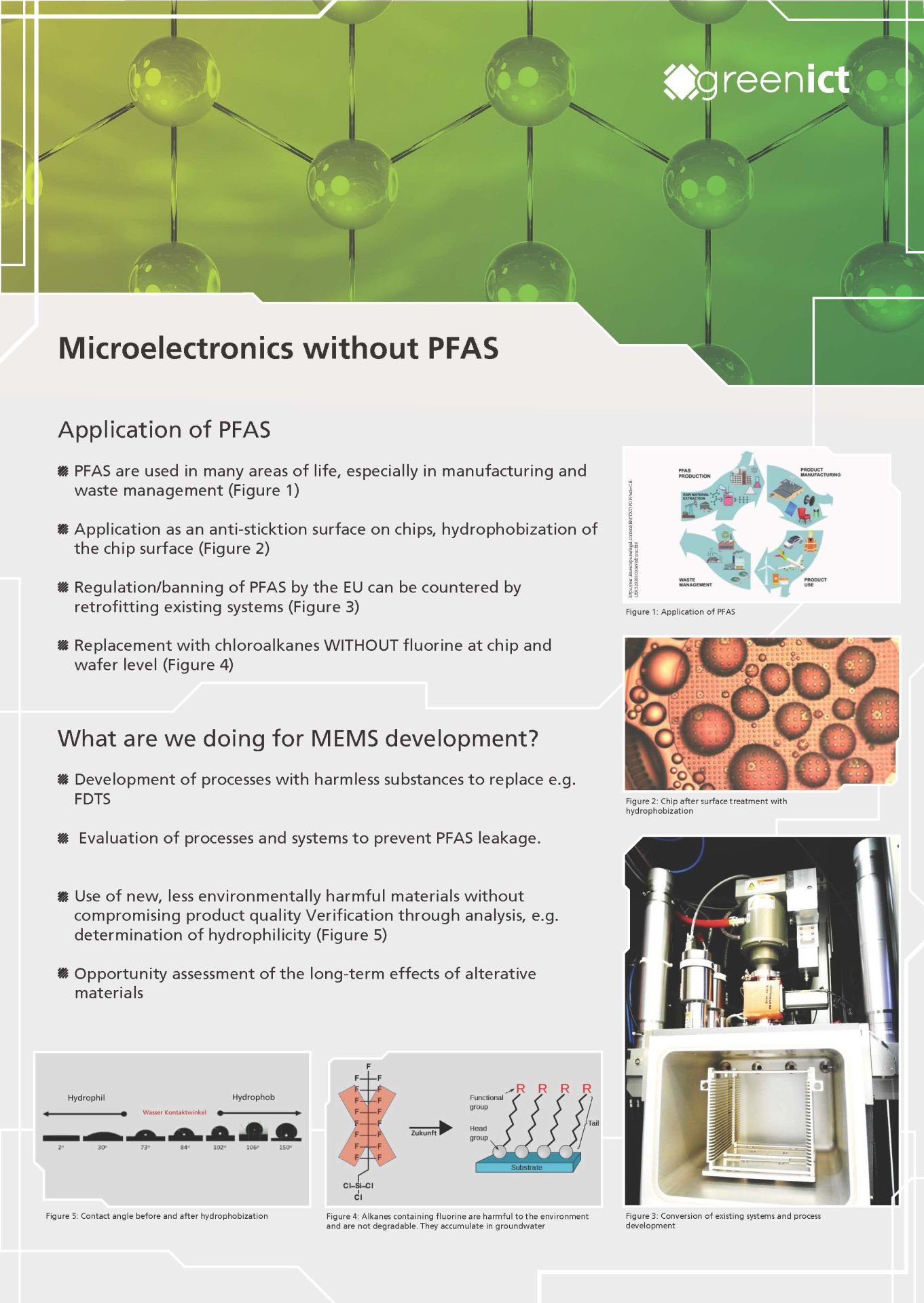
A central problem with MEMS components that are operated in air is the oxidation and moisture absorption of the active parts. To control this, PTFE (Teflon) is often used as a water-repellent layer.
To reduce or replace environmentally harmful materials in microelectronic processes, Fraunhofer IPMS is investigating whether the previously used PTFE can be replaced by FDTS without compromising the performance of ultrasonic devices (Capacitive Micro-machined Ultrasound Transducers, CMUT).
An important criterion for CMUTs is the resonant frequency and the pull-in voltages, which depend on the mechanical properties of the vibrating CMUT plate. The change from PTFE to FDTS influences these properties, which was investigated in detail.
PFAS replacement in ultrasonic sensors
Fraunhofer IPMS manufactures various CMUT versions that have different characteristics depending on the application. One of these applications is air-coupled CMUTs. In this design, the vibrating CMUT plate has holes to achieve additional damping by the air in the cavity and thus lower the resonant frequency. Lower frequencies result in better signal transmission and a longer range.
The directly deposited PTFE with a thickness of 100 nm was replaced by an ALD-processed FDTS with a thickness of only a few nanometers. This made it possible to achieve a uniform coating of the CMUTs. The previous PTFE had increased the vibrating mass and lowered the frequency. This frequency shift had to be investigated and adjusted. Sufficient statistical measurement data is available for the ultrasonic components with PTFE and FDTS. The resonant frequency increases by 4.4 % to 7.8 % by changing from PTFE to FDTS, depending on the design variant. This shift is shown in the wafer maps, which show the characterized CMUTs. The resonant frequencies are shown on the left with PTFE and on the right with FDTS. Three different designs were processed, which clearly show higher frequencies.
The expected shift can be transferred to similar designs by using alternative materials. FDTS is deposited using atomic layer deposition in an MVD300 system from SPTS. The design corrections have already been successfully implemented in several development projects for industrial customers. Major material changes require adjustments to the process, which can affect the function of the CMUTs. However, these changes can be compensated for by adjusting other design parameters.
Result
These measures have made it possible to significantly reduce the use of PFAS materials without impairing the function of the components. We are currently investigating which materials can be used as substitutes for FDTS in order to manufacture CMUTs completely without PFAS. These findings have been successfully transferred to other MEMS technologies at Fraunhofer IPMS.
 Fraunhofer Institute for Photonic Microsystems


