200 mm MEMS Processes

Wafer processes in our 200 mm cleanroom - precision and innovation


In our state-of-the-art 200 mm clean room, we offer comprehensive wafer processes that are tailored to the individual needs of our customers. We use our flexible and industry-compatible process line for this.

Our offering includes both complete processes and specialized individual processes to meet the most diverse requirements in MEMS, microdisplay and CMOS production, from front-end to back-end-of-line.

Our overall processes include surface micromachining, bulk micromachining and monolithic MEMS-on-CMOS integration as well as active silicon/electronic devices (CMOS). 

In addition, we offer a wide range of individual processes, including in particular silicon deep etching, various depositions (CVD to ALD), wafer bonding, dicing & packaging and inline characterization.

With state-of-the-art technology and an experienced team, we guarantee the highest quality and reliability in every step of the production process.

We offer you the following processes

Surface micromachining

Principle of surface micromachining
© Fraunhofer IPMS
Principle of surface micromachining
Process and technology capabilities in the field of surface micromechanics.
© Fraunhofer IPMS
Process and technology capabilities in the field of surface micromechanics.

Using sacrificial layer technology, Fraunhofer IPMS is able to manufacture actuators and sensors such as spatial light modulators (SLM) and capacitive ultrasonic sensors (CMUT). The processes and technology modules available to Fraunhofer IPMS for these highly complex components are:

  • PE-CVD for TEOS, HDP and a:Si.
  • Five-zone CMP for high planarity
  • Anti-stiction for excellent reliability
  • PVD for joints and mirrors with stress tuning
  • ALD for barrier coatings
  • Gas phase etching using HF and XeF2 for sacrificial layer processing
  • More: MEMS/MOEMS Process Developments and Tool Park

Bulk micromachining

Principle of bulk micromachining
© Fraunhofer IPMS
Principle of bulk micromachining
Process and technology capabilities in the field of bulk micromachining
© Fraunhofer IPMS
Process and technology capabilities in the field of bulk micromachining

Whether high-precision mirrors or the unique Nano-E-Drive principle developed by Fraunhofer IPMS: these actuators are based on deeply etched silicon structures with large aspect ratios (up to 40). In addition to the competencies in surface micromechanics, the following modules are available for further development:

  • Grinder for wafer thinning
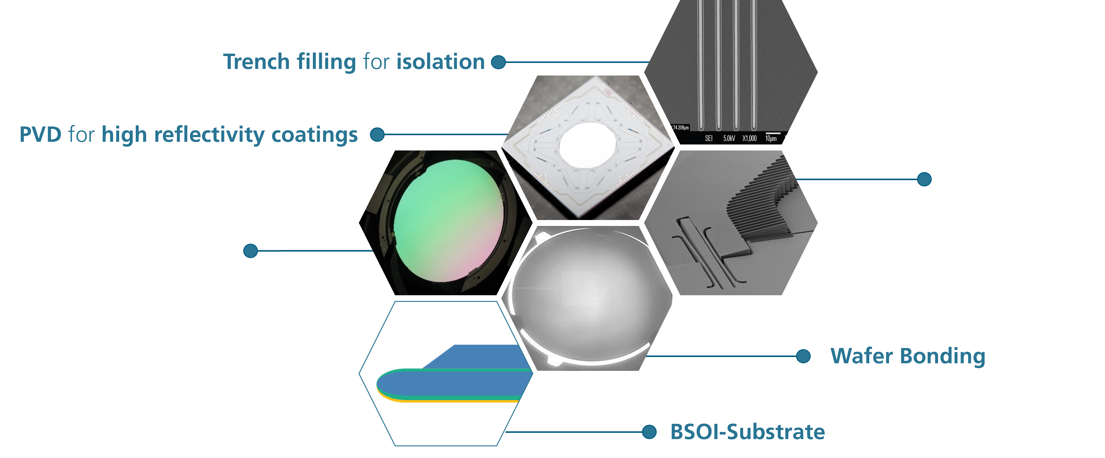
  • PVD for highly reflective layers
  • Wafer bonding for quasi-static motion
  • Deep silicon etching for the realization of comb drives
  • TMAH etching for backside openings
  • Trench backfill for insulation
  • B-SOI wafers as starting materials
  • More: Mechanical Actuators

Monolithic MEMS-on-CMOS Integration

Integration of MEMS on CMOS
© Fraunhofer IPMS
Integration of MEMS on CMOS
Development of MEMS-on-CMOS Technologies
© Fraunhofer IPMS
Development of MEMS-on-CMOS Technologies

Monolithic integration of MEMS on CMOS is an integration technology for the fabrication of wafer-level integrated systems. Fraunhofer IPMS develops and manufactures monolithically integrated MEMS to minimize parasitic effects. With this technology, especially large devices with a high integration density can be realized reliably. Examples are SLMs, thermopile and CMUT arrays.

Active Silicon / Electronic Devices

© Fraunhofer IPMS
Ion-sensitive field-effect transistor of the Fraunhofer IPMS

Fraunhofer IPMS manufactures wafer-level devices that utilize the chemical and physical properties of functional layers, e.g. in ion-sensitive field-effect transistors (ISFET) for measuring pH values.

  • Thermal oxidation for gate oxides (SiO2)
  • Deposition of active layers (e.g. Nb2O5)
  • More: Chemical Sensors

We offer you the following single processes

Deep silicon etching

© Fraunhofer IPMS

Silicon deep etching (Bosch process) is one of the core competencies in our clean room at Fraunhofer IPMS. This highly precise and repeatable etching process enables the fabrication of deep, anisotropic structures in silicon substrates, which are essential for a variety of applications in micro- and nanotechnology.

Our state-of-the-art equipment and experienced team ensure that the most complex designs are realized with the highest accuracy and consistency.

Deposition

© Fraunhofer IPMS
  • Atomic Layer Deposition ALD
  • LP-CVD 
  • PE-CVD
  • PVD sputtering
  • Evaporation
  • Oxidation
  • Rapid Thermal Annealing
  • Vapor phase deposition

Wafer Bonding, Dicing & Packaging

© Fraunhofer IPMS
Pick and place of a spatial light modulator (SLM)
  • Direct bonding (Si / SiO2 , Si / Si and plasma-assisted bonding).
  • Adhesive bonding (BCB bonding)
  • Thermocompression bonding
  • SOI-design and manufacturing
  • Dicing of glass-silicon compounds
  • Fineplacer

Inline Characterization

© Fraunhofer IPMS
  • Optical coating thickness measurement
  • Inline reflectance measurement
  • Scanning electron microscopy
  • CD-SEM
  • Atomic Force Microscopy
  • Ellipsometry
  • White light inferometer
  • Laser scanning microscopy
  • Defect measurements
  • Ultra-high frequency vibrometry