TO.QI - Semiconductor technology modules for quantum computing, AI and Internet-of-Things

Semiconductor technology modules for quantum computing, AI and the Internet of Things (TO.QI)

Project duration: 2024 - 2027

© Fraunhofer IPMS
Overview of the technology modules of the TO.QI project (technologies in gray are not part of the project).

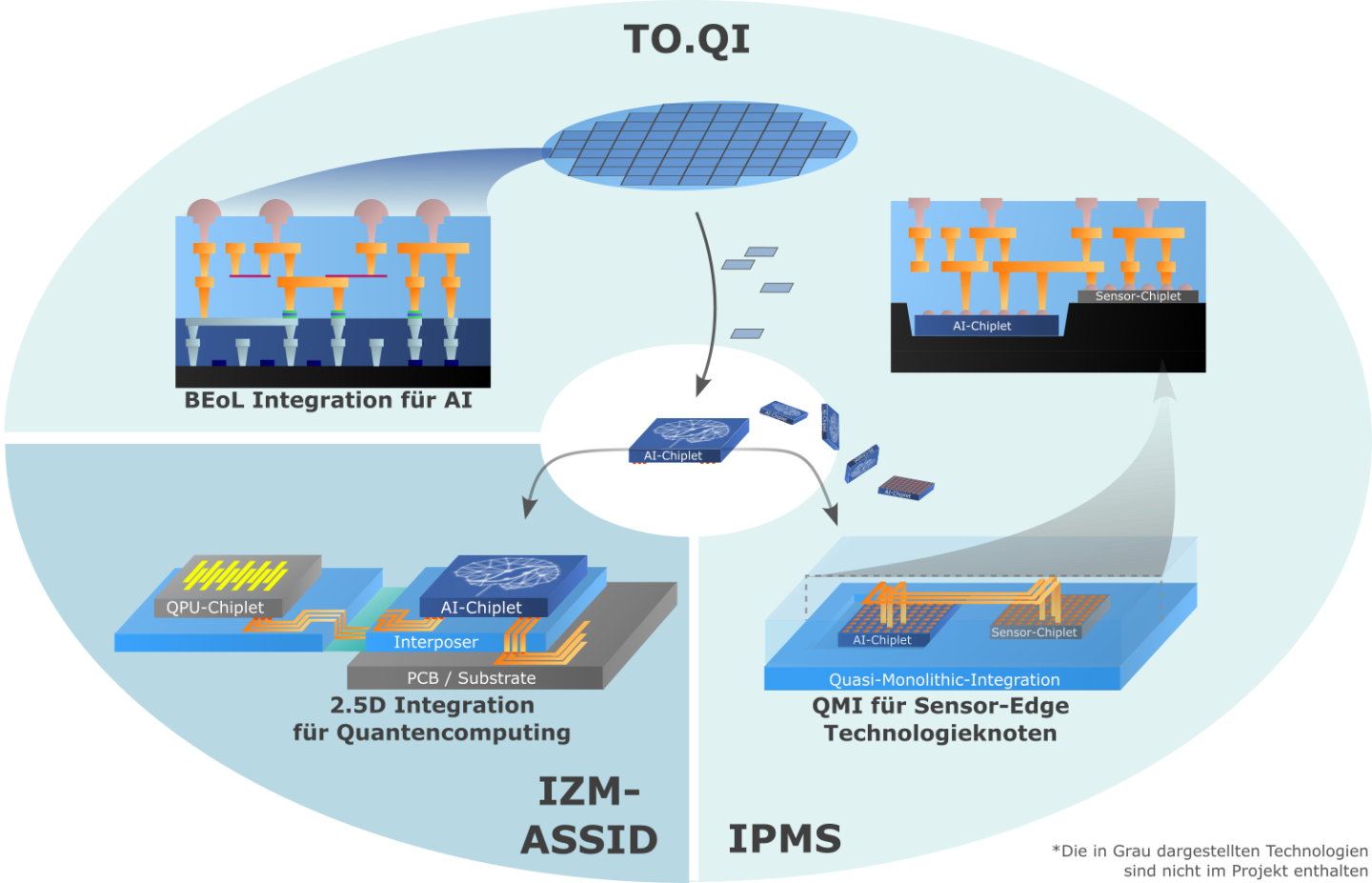
The rapidly growing demand for computing power, particularly in relation to quantum computing, artificial intelligence and “Internet of Things” (IoT) applications, urgently requires new microelectronics solutions to counteract the associated drastic increase in energy consumption and reduce greenhouse gas emissions. One promising solution for this is new computing architectures based on non-volatile memory components, which enable compute-in-memory / neuromorphic computing, as well as the most compact possible integration of different systems. The latter can be achieved through heterointegration. 3D integration via an interposer or the quasi-monolithic integration of several chiplets are particularly promising for quantum computing systems and IoT sensor edge solutions.

The aim of the TO.QI project is therefore to develop such technology modules, which should enable research-oriented pilot production of new components and heterointegration methods. Accordingly, the project is divided into three sections, with two technology modules being developed by Fraunhofer IPMS and one technology module by Fraunhofer IZM-ASSID.

© Fraunhofer IPMS
Schematic representation of the technologies to be integrated into the BEoL in Technology Module 1.

Technology module 1): BEoL (Back-End-of-Line) integration for AI

Development of a BEoL module that can be placed on an existing commercial front-end-of-line CMOS wafer. This module contains novel components such as ferroelectric capacitors and thin-film resistors, which are required for AI (Artificial Intelligence) hardware accelerators in edge AI applications. The resulting AI chiplet can be used for heterointegration.

Ferroelectric non-volatile memory components, in particular BEoL-integrated ferroelectric capacitors, are used to realize an AI chiplet with particularly low power consumption. Thin-film resistors will ensure improved current variability and the components will be optimized for ultra-low power and high speed. The modular PDK developed for this purpose can be used in future by SMEs/IDMs to realize chiplet/interposer development and pilot production based on novel components.

© Fraunhofer IPMS
Schematic representation of the technologies to be developed for the quasi-monolithic integration of chiplets (technologies shown in gray are not part of the TO.QI project).

Technology module 2): Quasi-monolithic integration (QMI) for sensor edge technology nodes

Development of a QMI integration process for sensor edge applications, for example in the automotive sector. This represents a use case for edge applications of the AI chiplet (e.g. for autonomous driving).

Quasi-monolithic integration is a new, innovative integration principle for ultra-high chiplet density by integrating very thin chiplets into the surface of a carrier (e.g. interposer) in such a way that a BEoL module (see technology module 1) can subsequently be used for high-density wiring of the chiplets. This form of integration allows highly integrated chiplet systems to be realized, e.g. also the combination of AI chiplets from technology module 1 with sensors. The integration module is developed in this technology module (TRL4) and validated using a sensor demonstrator

© Fraunhofer IPMS
Schematic diagrams of the technologies being developed in Technology Module 3 of the TO.QI project (technologies shown in gray are not part of the project).

Technology module 3): 2.5D integration for quantum computing (QC) 

Development of an interposer for a cryogenic (low temperature) environment, which enables two thermally decoupled areas by means of a flexible connection. This represents a use case for quantum error correction of the AI chiplet and advantages over classical quantum computing integrations. In addition, Fraunhfofer IPMS supports the developments in TM3 at Fraunhofer IZM-ASSID with electrical measurements in the cryogenic temperature range as well as UBM processes and layout of test structures/interfaces.

Supported by: