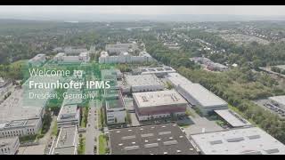
The Fraunhofer Institute for Photonic Microsystems IPMS in Dresden is your access to know-how, expertise and modern R&D infrastructure in the field of optical sensors and actuators, integrated circuits, microsystems (MEMS/MOEMS) and nanoelectronics.
Fraunhofer IPMS is one of currently 75 institutes and research institutions of the Fraunhofer-Gesellschaft, the world’s leading applied research organization. With its focus on developing key technologies that are vital for the future and enabling the commercial exploitation of this work by business and industry, Fraunhofer plays a central role in the innovation process. As a pioneer and catalyst for groundbreaking developments and scientific excellence, Fraunhofer helps shape society now and in the future. The majority of the organization’s 30,000 employees are qualified scientists and engineers, who work with an annual research budget of 2.8 billion euros. Of this sum, 2.3 billion euros is generated through contract research. Around 70 percent of this sum are generated through industrial commissions and publicly financed research projects. The remainder is contributed by the Federal Government and the Länder as basic funding.
Fraunhofer IPMS is part of the Fraunhofer Group for Microelectronics, the Research Fab Microelectronic Germany, and is engaged in various regional and international networks in the filed microsystems and photonics.
In order to meet the challenging demands of our customers, the Fraunhofer IPMS is certified according to the standard DIN EN 9001:2015 for research, development and fabrication of photonic microsystems including semiconductor and microsystem processes as well as integrated actuators and sensor technologies.
The Institute has Four Locations:
Our headquarter is located at Maria-Reiche-Straße 2 in Dresden, Germany. With its 1500 m² clean room, it is at your service for all your technology development requirements, as well as for pilot production. Commissioned and online beginning in September 2007, our MEMS and CMOS facility is rated at Class 4 per ISO 14644-1, or Class 10 per U.S. Standard 209E.
The division »Center Nanoelectronic Technologies« has its own cleanroom infrastructure for process and material development on 300 mm wafers with the branch office "An der Bartlake 5" in the immediate vicinity of the chip producer Globalfoundries. For processing customer orders, 2700 m² of clean room space of class 6 and 3 (according to ISO 14644-1) as well as laboratory space for more than 80 processing and analytical tools are available. The equipment park includes deposition and etching systems as well as inspection and analysis equipment for determining defects and measuring layer properties.
At the Cottbus branch »Integrated Silicon Systems« we work on monolithic integrated actuator and sensor systems as well as on terahertz micro modules and applications.
In the Fraunhofer Center Erfurt we focus on innovative systems for biomedical applications together with the Fraunhofer Institutes IOF and IZI.

 Fraunhofer Institute for Photonic Microsystems


