Devices

Hyperspectral imaging inspection tool for efficient semiconductor production

© DIVE imaging systems Gmbh

Together with DIVE Imaging Systems GmbH, we are working in the GreenICT Space of the GreenICT@FMD competence center on the introduction of hyperspectral imaging technology as a screening tool for semiconductor production. The aim is to make production processes more efficient and sustainable by detecting defects at an early stage and conserving resources. This not only improves environmental compatibility, but also reduces the costs of semiconductor production. The project shows how sustainable solutions in microelectronics can be realized through innovative technologies and cooperation.

Low power chips for digital, analog and high-frequency technologies

The aim is to develop energy-efficient chips for digital, analog and high-frequency applications. The FAMES pilot line will drive forward five new technologies: FD-SOI with two new nodes at 10nm and 7nm, various types of embedded non-volatile memory such as OxRAM, FeRAM, MRAM and FeFETs, as well as high-frequency components such as switches, filters and capacitors. In addition, two 3D integration options - heterogeneous and sequential integration - are being developed, complemented by small inductors for the production of DC-DC converters for power supply integrated circuits (PMIC).

Resource- and energy-saving ISFET-based sensor technology

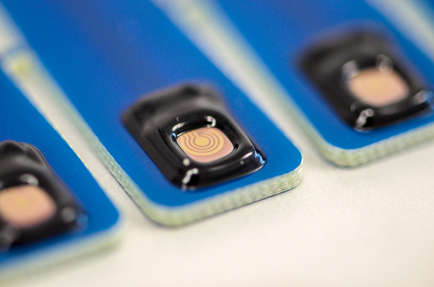
The research aims to develop resource-saving processes in sensor technology, particularly for ISFETs for pH sensors. Tantalum, an expensive and critical material, is often used in high-performance pH measurement technology. Alternatives often offer sufficient performance at lower cost and energy savings in processing. Another focus is on the resource-saving characterization and integration of ISFETs, avoiding conventional bonding processes and materials such as palladium or silver alloys. New methods are being developed for sensor functionalization that minimize material losses. Instead of flat coatings, in which more than 99% of the material is lost, the aim is direct structuring at wafer level using microfine dispensing. This reduces material consumption, saves on reactive and toxic substances, reduces health risks for employees and protects the environment.

Neuromorphic Computing

Increasing digitalization is placing growing demands on electronic hardware in applications such as Industry 4.0, smart cities and autonomous driving. Speed, miniaturization and energy efficiency are key factors, especially in data-intensive areas such as big data analysis and artificial intelligence (AI). Neuromorphic computing is an innovative approach to overcoming these challenges. This technology imitates the self-organizing and adaptive functioning of the human brain and thus enables high-performance and energy-efficient applications.

Fraunhofer IPMS is developing specialized materials, technologies and complete hardware solutions that are particularly optimized for use in the edge area - for example in intelligent sensors and decentralized systems that can process data and make decisions independently.