 Fraunhofer Institute for Photonic Microsystems
Photonic Biosensors
Photonic biosensors are very well suited for rapid and accurate molecular analysis in point-of-care applications for early detection of diseases, as an alternative to the standard method of detecting microorganisms by blood cultures, for food analysis or for environmental monitoring.
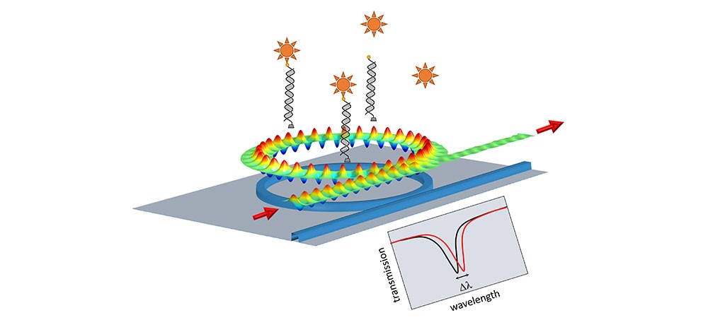
We are developing photonic biosensors with silicon nitride microring resonators as transducer elements. In detail, the microring resonator-based biosensor works as follows: Target bioproteins that bind to the surface of the functionalised microring structure cause a change in the effective refractive index of the mode entering the structure and thus a shift in the resonance wavelength, which is detected when monitoring the spectrum at the output port. The narrower the resonance peaks of the transmission spectrum, the higher the sensitivity of the resonator.
Furthermore, a suitable functionalisation of the microring surface enables the detection of a binding between a specific bioactive receptor (antibody, DNA) and the analyte (e.g. biomarker protein) that takes place on the modified surface. Micro-ring resonator-based biosensors could be used to detect biomarker proteins down to very low concentrations of about 10 pg/ml.
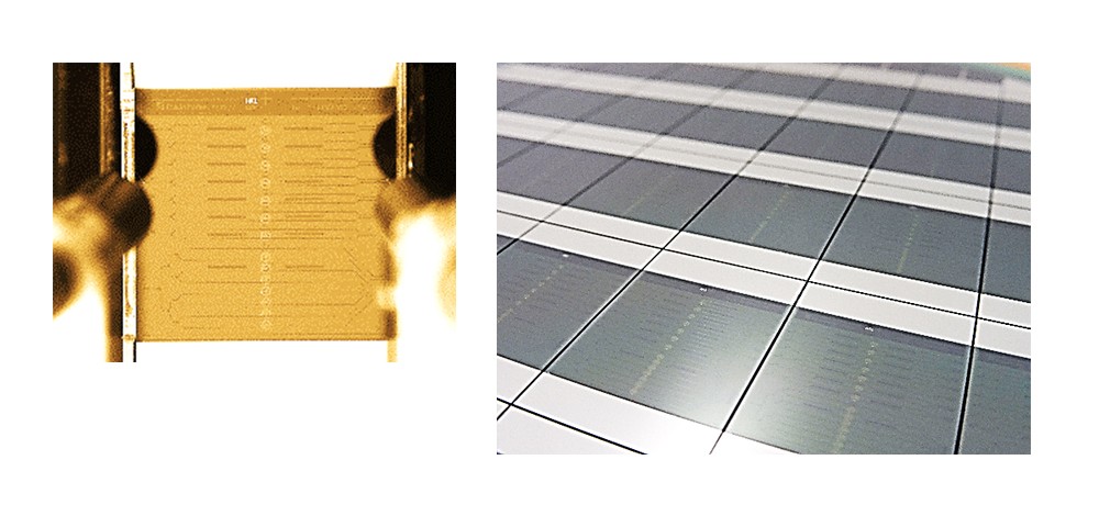
We are developing a highly sensitive, cost-effective, reliable and scalable on-chip biosensor platform with multiplex architecture and optimised light coupling to the chip.
