Motivation
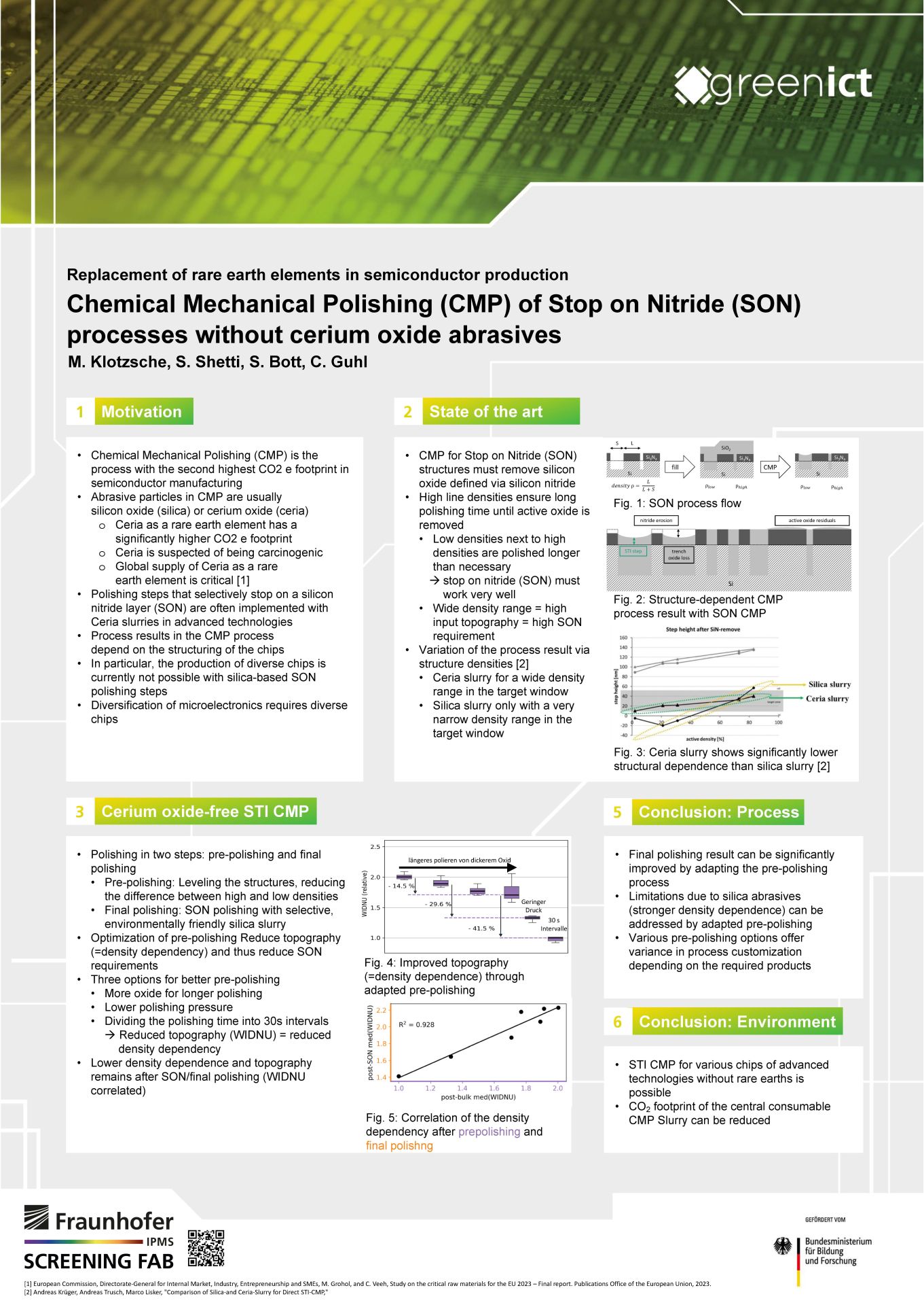
Chemical Mechanical Polishing (CMP) is a critical process in semiconductor manufacturing, but it is also one of the processes with the second highest CO2 footprint. The abrasive particles used are usually silicon oxide (silica) or cerium oxide (ceria). Ceria, a rare earth element, causes a significantly higher CO2 footprint and is also suspected of being carcinogenic. The global supply of ceria is critical.
In advanced technologies, polishing steps that selectively stop on a silicon nitride (SON) layer are often performed with ceria slurries. The results of the CMP process are highly dependent on the patterning of the chips. Currently, the production of diverse chips with silica-based SON polishing steps is not possible, which limits the diversification of microelectronics and increases the need for different chip designs.
State of the art
In chemical mechanical polishing (CMP) for stop on nitride (SON) structures, it is necessary to precisely remove silicon oxide via silicon nitride. High line densities lead to longer polishing times until the active oxide is completely removed. In areas with low densities next to high densities, polishing times may be longer than necessary, emphasizing the need for excellent functionality of the SON.
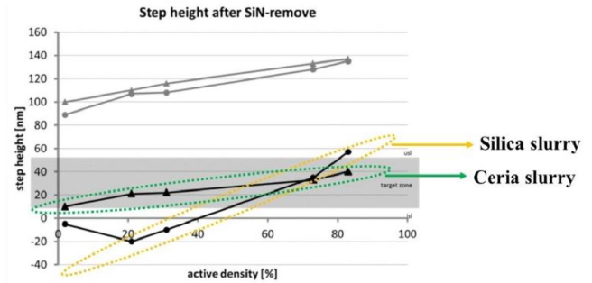
A wide density range results in a high input topography, which increases the demands on the SON. There is a variation in process results depending on the structure densities. For a wide density range within the target window, a Ceria slurry is required, while a Silica slurry can only be used for a very narrow density range in the target window.
 Fraunhofer Institute for Photonic Microsystems


